Jul. 6, 2012 Research Highlight Chemistry Physics / Astronomy
Organic electronics edge closer
A self-assembled organic superstructure formed on a gold electrode displays rare, and potentially useful, semiconducting properties
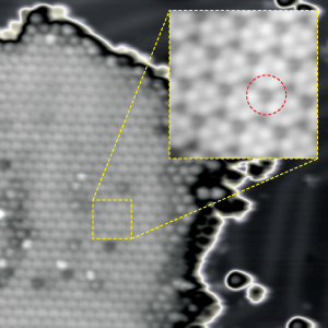 Figure 1: A scanning tunneling microscopy image reveals the homogeneous pattern of fluorinated fullerene molecules (one molecule is circled) that form on the surface of a gold electrode. Reproduced, with permission, from Ref. 1 © 2012 American Chemical Society
Rays of sunshine bathe our planet in reliable and free renewable energy; yet, harnessing this energy remains a costly process because today’s solar cells depend upon expensive materials to capture light. An emerging solar technology based on cheap organic materials could one day offer an attractive alternative, and potentially make solar cells affordable enough to install on every rooftop. Such low-cost solar cells are just one example of the organic electronic devices that could result from the joint research of Yousoo Kim at the RIKEN Advanced Science Institute (ASI) in Wako and Maki Kawai at the University of Tokyo.
Kim and Kawai’s team is exploring the electronic properties of thin films of organic molecules derived from soccer-ball-shaped structures of carbon atoms, called fullerenes. These molecules are covered with delocalized electrons, giving them potentially useful electronic properties that can be fine-tuned by modifying the fullerene’s structure. Attaching fluorine atoms to the fullerene is a particularly attractive method for tuning these attributes, as the resulting fluorinated fullerenes should show a useful semiconducting behavior, known as ‘n-type behavior’, which is rare in organic materials. However, to date, the resulting materials have proved difficult to study, owing to their structural complexity, and tendency to form as mixtures.
By coating gold electrode surfaces with an ultra-thin layer of fluorinated fullerenes in the form of a powder, Kim, Kawai and their colleagues studied the properties of fluorinated fullerenes in detail using scanning tunneling microscopy (STM)1. They found that when they deposited the powder onto the gold at room temperature, fluorinated fullerene islands—just a single molecule thick—formed in patches across the gold surface. However, the orientation of molecules in these patches was jumbled, and the electronic properties of each island were inhomogeneous.
When they gently warmed the gold surface, however, a very different picture emerged from the STM images: the islands had assembled into uniform films in which all molecules oriented in the same manner, with homogeneous electric behavior.
Mastering the monolayer
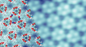 Figure 2: Computational calculations show that intermolecular interactions (arrows) drive the fluorinated fullerenes to self-assemble precisely on a gold surface (underlying grid). Reproduced, with permission, from Ref. 1 © 2012 American Chemical Society
“We were very surprised by the well-ordered monolayer that formed on the gold surface,” says Tomoko Shimizu, a member of the team based at RIKEN ASI. To investigate how the homogeneous fluorinated fullerene film formed, she and her colleagues first determined its exact molecular composition—a process complicated by the impurity of the fluorinated fullerene powder. Although each fluorinated fullerene was coated with precisely 36 fluorine atoms, these atoms could be distributed in different patterns across the fullerene surface. This formed three different fluorine distributions, or isomers: C3, C1 and T.
“When I first saw the well-ordered structure in the STM images, I thought it was a mixture of the three isomers,” Shimizu says. However, subsequent computer modeling studies revealed otherwise. Through the scanning tunneling microscope, each molecule in the homogenous region had an identical appearance—a dark spot surrounded by six bright lobes, arranged in a roughly hexagonal shape (Fig. 1).
Kim, Kawai and colleagues used density functional theory (DFT) calculations to predict how each isomer would orient on the gold surface, and therefore appear under a scanning tunneling microscope. The calculations predicted that each isomer should look quite different; however, each molecule in the STM images of the homogenous regions looked identical. By comparing these images with the structures predicted by DFT, the researchers concluded that the monolayer consisted exclusively of the C3 isomer—the only isomer predicted to align itself directionally on the gold. “Nature is great; the molecules have filtered themselves though a self-assembling process,” says Shimizu.
Further calculations revealed that attractive forces between neighboring fluorinated fullerene molecules drove the selective self-assembly process. When a fullerene is decorated with fluorine atoms, the molecular surface consists of an electron-rich and an electron-poor region because of the strong electron-withdrawing property of fluorine atoms. As the researchers heated the gold, the fluorinated fullerenes reoriented in a way that maximized the attractive forces between the fluorine atoms on one molecule and the delocalized electrons on part of the next molecule (Fig. 2).
Applications beckon
The self-assembling fluorinated fullerene monolayer showed electronic properties that are particularly promising for future applications in organic electronic devices ranging from computers to television screens to solar cells. The fluorinated fullerene–gold superstructure exhibits semiconductor behavior, a property that underpins such devices. The semiconductor industry is currently dominated by expensive semiconducting silicon wafers. Organic alternatives would not only be cheaper, they would also be ultra-thin, light-weight and flexible.
Most electronic devices need pairs of semiconductor materials in order to function: n-type semiconductors, which are rich in electrons; and p-type, which are electron poor. Thus far, this need for pairing has limited the uptake of organic semiconductors. Despite the availability of p-type organic semiconductors, n-type organic materials are rare. “Our fluorinated fullerene monolayer has a perfectly homogeneous structure and electronic properties all over the well-ordered superstructure area, and indeed n-type behavior on a chemically stable gold electrode, making it potentially useful for organic devices,” says Shimizu.
Inexpensive solar cells are undoubtedly one area that could benefit from the researchers’ novel material. Most solar cells use a ‘p–n junction’ to funnel electrons, which have been knocked free by incoming light, out of the cell and around an electrical circuit. This is one of the potential applications that the researchers plan to investigate first. “There are a few possibilities for our next step in this area,” says Shimizu. “One is to study structure and energy level alignment of organic p–n junctions with and without light irradiation for solar cell applications.”
References
- 1. Shimizu, T.K., Jung, J., Otani, T., Han, Y.-K., Kawai, M. & Kim, Y. Two-dimensional superstructure formation of fluorinated fullerene on Au(111): A scanning tunnelling microscopy study. ACS Nano 6, 2679–2685 (2012). doi: 10.1021/nn300064x
About the Researcher
Tomoko Shimizu

Tomoko Shimizu was born in Saitama, Japan, in 1979. She graduated from the Faculty of Science and Technology, Keio University in 2002, and obtained her PhD in 2007 from the Department of Materials Science and Engineering at the University of California, Berkeley, USA. At Berkeley, Shimizu worked on the instrumentation of scanning probe microscopy and performed research in the field of surface science for catalysis and the environmental sciences. She returned to Japan as a research associate in 2007 and became a special postdoctoral researcher in 2009 in the Surface Chemistry Laboratory at RIKEN. Shimizu then transferred to the Surface and Interface Science Laboratory at RIKEN in 2010, and was promoted to scientist at the Advanced Science Institute in 2012. Her research focuses on the structure and electronic properties of atoms and molecules as well as the defects of various types of surfaces using scanning tunneling microscopy and atomic force microscopy.