May 18, 2020 Press Release Physics / Astronomy
“Tantalizing” clues about why a mysterious material switches from conductor to insulator
Tantalum disulfide is a mysterious material. According to textbook theory, it should be a conducting metal, but in the real world it acts like an insulator. Using a scanning tunneling microscope, researchers from the RIKEN Center for Emergent Matter Science have taken a high-resolution look at the structure of the material, revealing why it demonstrates this unintuitive behavior.
It has long been known that crystalline materials should be good conductors when they have an odd number of electrons in each repeating cell of the structure, but may be poor conductors when the number is even. However, sometimes this formula does not work, with one case being “Mottness,” a property based on the work of Sir Nevill Mott. According to that theory, when there is strong repulsion between electrons in the structure, it leads the electrons to become “localized”—paralyzed in other words—and being unable to move around freely to create an electric current. What makes the situation complicated is that there are also situations where electrons in different layers of a 3-D structure can interact, pairing up to create a bilayer structure with an even number of electrons. It has been previously suggested that this “pairing” of electrons would restore the textbook understanding of the insulator, making it unnecessary to invoke “Mottness” as an explanation.
For the current study, published in Nature Communications, the research group decided to look at tantalum disulfide, a material with 13 electrons in each repeating structure, which should therefore be a conductor. However, it is not, and there has been controversy over whether this property is caused by its “Mottness” or by a pairing structure.
To perform the research, the researchers created crystals of tantalum disulfide and then cleaved the crystals in a vacuum to reveal ultra-clean surfaces which they then examined, at a temperature close to absolute zero—with a method known as scanning tunneling microscopy—a method involving a tiny and extremely sensitive metal tip that can sense where electrons are in a material, and their degree of conducting behavior, by using the quantum tunneling effect. Their results showed that there was indeed a stacking of layers which effectively arranged them into pairs. Sometimes the crystals cleaved between the pairs of layers, and sometimes through a pair, breaking it. They performed spectroscopy on both the paired and unpaired layers and found that even the unpaired ones are insulating, leaving Mottness as the only explanation.
According to Christopher Butler, the first author of the study, “The exact nature of the insulating state and of the phase transitions in tantalum disulfide have been long-standing mysteries, and it was very exciting to find that Mottness is a key player, aside from the pairing of the layers. This is because theorists suspect that a Mott state could set the stage for an interesting phase of matter known as a quantum spin liquid.”
Tetsuo Hanaguri, who led the research team, said, “The question of what makes this material move between insulating to conducting phases has long been a puzzle for physicists, and I am very satisfied we have been able to put a new piece into the puzzle. Future work may help us to find new interesting and useful phenomena emerging from Mottness, such as high-temperature superconductivity.”
Reference
- Butler C J, Yoshida M, Hanaguri T, and Iwasa Y (2020). Mottness versus unit-cell doubling as the driver of the insulating state in 1T-TaS2. Nature Communications doi: 10.1038/s41467-020-16132-9
Contact
Team Leader
Tetsuo Hanaguri
Emergent Phenomena Measurement Research Team
RIKEN Center for Emergent Matter Science
Special Postdoctoral Researcher
Christopher Butler
Emergent Phenomena Measurement Research Team
RIKEN Center for Emergent Matter Science
Jens Wilkinson
RIKEN International Affairs Division
Tel: +81-(0)48-462-1225 / Fax: +81-(0)48-463-3687
Email: pr [at] riken.jp
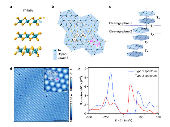
Overview of charge order, inter-layer stacking and cleaved surfaces in 1T-TaS2. a The quasi-2D undistorted structure of 1T-TaS2. b The supercell describing the periodic SD distortion within a single 1T-TaS 2 layer. The teal and blue rhombuses mark the 2D projections of the undistorted atomic unit cell, and the supercell after onset of the commensurate CDW, respectively. The labels A, B, and C denote the possible sites atop which successive SD clusters can stack. c The SD stacking pattern currently discussed (S not shown), with two SDs per cell and two distinct cleavage planes, 1 and 2. d Typical STM topography taken at a vacuum-cleaved 1T-TaS 2 surface (V = 250 mV, Iset = 500 pA, scale bar 20 nm). The inset shows the correspondence between the topographic modulation and the SD cluster lattice (scale bar 1 nm). e Examples of conductance spectra of the two types observed at multiple cleaved surfaces. Typically, one type of spectrum or the other appears uniformly (except in the vicinity of defects) over approx. 1 μm areas, unless a step-terrace morphology is observed. It will be shown below that the type 1 and 2 spectra correspond to surfaces formed by cleavage at planes 1 and 2 respectively.
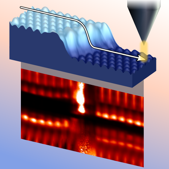
The experimental setup