Dec. 23, 2021 Press Release Engineering
Fabrication of flexible electronics improved using gold and water-vapor plasma
Researchers at the RIKEN Center for Emergent Matter Science (CEMS) and the RIKEN Cluster for Pioneering Research (CPR) in Japan have developed a technique to improve the flexibility of ultra-thin electronics, such as those used in bendable devices or clothing. Published in Science Advances, the study details the use of water vapor plasma to directly bond gold electrodes fixed onto separate ultra-thin polymer films, without needing adhesives or high temperatures.
As electronic devices get smaller and smaller, and the desire to have bendable, wearable, and on-skin electronics increases, conventional methods of constructing these devices have become impractical. One of the biggest problems is how to connect and integrate multiple devices or pieces of a device that each reside on separate ultra-thin polymer films. Conventional methods that use layers of adhesive to stick electrodes together reduce flexibility and require temperature and pressure that are damaging to super-thin electronics. Conventional methods of direct metal-to-metal bonding are available, but require perfectly smooth and clean surfaces that are not typical in these types of electronics.
A team of researchers led by Takao Someya at RIKEN CEMS/CPR has developed a new method to secure these connections that does not use adhesive, high temperature, or high pressure, and does not require totally smooth or clean surfaces. In fact, the process takes less than a minute at room temperature, followed by about a 12-hour wait. The new technique, called water-vapor plasma-assisted bonding, creates stable bonds between gold electrodes that are printed into ultra-thin—2 thousandths of a millimeter!—polymer sheets using a thermal evaporator.
“This is the first demonstration of ultra-thin, flexible gold electronics fabricated without any adhesive,” says Senior Research Scientist Kenjiro Fukuda of RIKEN CEMS/CPR. “Using this new direct bond technology, we were able to fabricate an integrated system of flexible organic solar cells and organic LEDs.” Experiments showed that water-vapor plasma-assisted bonding performed better that conventional adhesive or direct bonding techniques. In particular, the strength and consistency of the bonds were greater than what standard surface-assisted direct bonding achieved. At the same time, the material conformed better to curved surfaces and was more durable than what could be achieved using a standard adhesive technique.
According to Fukuda, the method itself is surprisingly simple, which might explain why they discovered it by accident. After fixing the gold electrodes onto polymer sheets, a machine is used to expose the electrode sides of the sheets to water-vapor plasma for 40 seconds. Then, the polymer sheets are pressed together so that the electrodes overlap in the correct location. After waiting 12 hours in room temperature, they are ready to use. Another advantage of this system is that after activation with water-vapor plasma, but before being bonded together, the films can be stored in vacuum packs for days. This is an important practical aspect when considering the potential for ordering and distributing pre-activated components.
As proof of concept, the team integrated ultra-thin organic photovoltaic and LED-light modules that were printed on separate films and connected by five additional polymer films. The devices withstood extensive testing, including being wrapped around a stick and being crumpled and twisted to extremes. Additionally, the power efficiency of the LEDs did not suffer from the treatment. The technique was also able to join pre-packaged LED chips to a flexible surface.
“We expect this new method to become a flexible wiring and mounting technology for next-generation wearable electronics that can be attached to clothes and skin,” says Fukuda. “The next step is to develop this technology for use with cheaper metals, such as copper or aluminum.”
Reference
Contact
Kenjiro Fukuda and Takao Someya
Thin-Film Device Laboratory
Cluster for Pioneering Research
and
Emergent Soft System Research Team
Center for Emergent Matter Science (CEMS)
Adam Phillips
RIKEN International Affairs Division
Tel: +81-(0)48-462-1225
Email: gro-pr [at] riken.jp
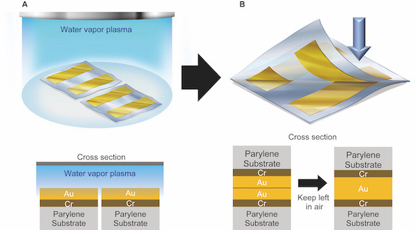
Fig 1. Schematic
(A) Evaporated gold surfaces on 2 μm thick parylene substrates were exposed to water vapor plasma. (B) Bonding of water vapor plasma treated-gold was achieved by overlapping the two substrates and storing them in ambient air for a few seconds to several hours without any applied pressure or heat.

Fig 2. Example device.
An OPV, an OLED, and five wiring films were fabricated on different ultra-thin substrates and then integrated using WVPAB. On the right, the integrated system is being wrapped around a stick (radius of 10 mm).

Fig 3. Conformability test.
Images from the conformability test on a curved surface (radius: 0.5 mm). Ultra-thin films bonded using (top) water-vapor plasma assisted bonding or (bottom) standard adhesive. Conformability was much better for water-vapor plasma assisted bonding.